In-Vision supports quest to develop revolutionary sub-micron resolution 3D-printing process
As electronic devices become more and more miniaturised, the demand for smaller optical components creates production challenges. Conventional methods for 3D-printing of sub-micron sized photonic devices is, in most cases, very costly and impractical outside of a laboratory. Read how In-Vision is helping to overcome this challenge.
To overcome this challenge, Professor Tapajyoti Das Gupta of the Indian Institute of Science-Bangalore is pushing the boundaries of 3D-printing by developing a new printer capable of delivering sub-micron resolution to produce flexible, stretchable photonic devices with the potential to disrupt the entire semiconductor industry and build a more resilient supply chain.
Demand for Devices Creates Production Hurdles
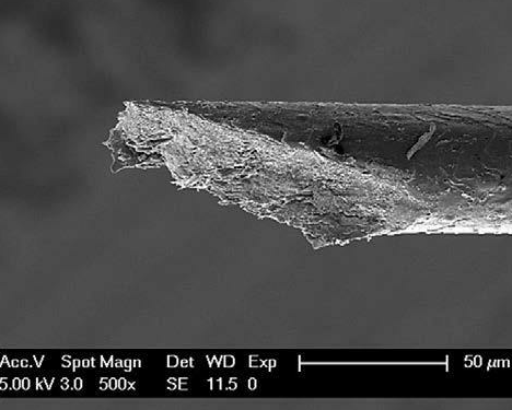
High-performance optical devices are everywhere: from the average smartphone camera to augmented reality and virtual reality equipment, we’ve become accustomed to and demand exceptional quality imaging capabilities in increasingly smaller form factors. The problem is, producing these precision nanostructures typically requires a multi-step, layered 2D lithography process that requires multiple machines in a cleanroom facility, which makes it costly and hinders scalability.
Aiming to accelerate production and lower the cost, Das Gupta is working with In-Vision and J Group Robotics to build the first large format, sub-micron resolution 3D printer to produce exceptional quality optical devices faster and more economically than current 3D-printing technology allows. By eliminating the clean room and simplifying the process into one machine rather than 10, Das Gupta and his team are opening the doors to much greater production scale and new and broader applications.
In-Vision Light Engine Delivers Sub-Micron Resolution
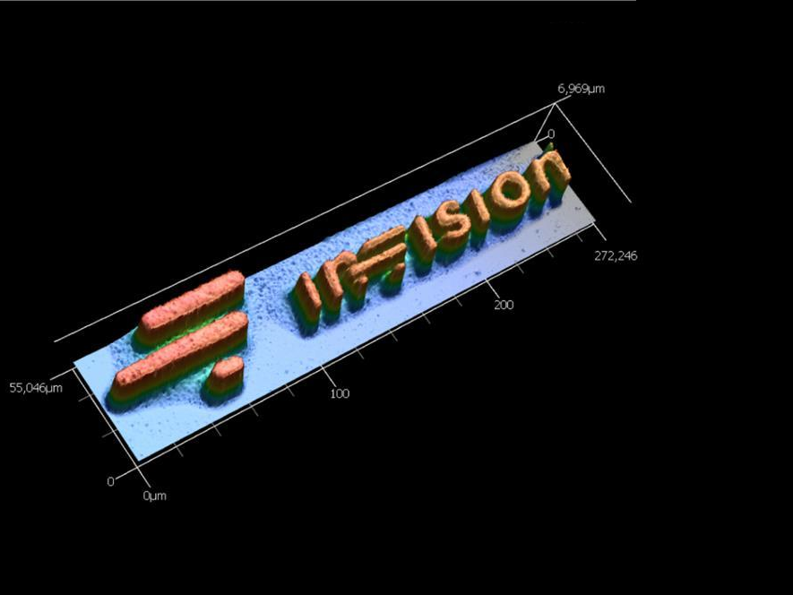
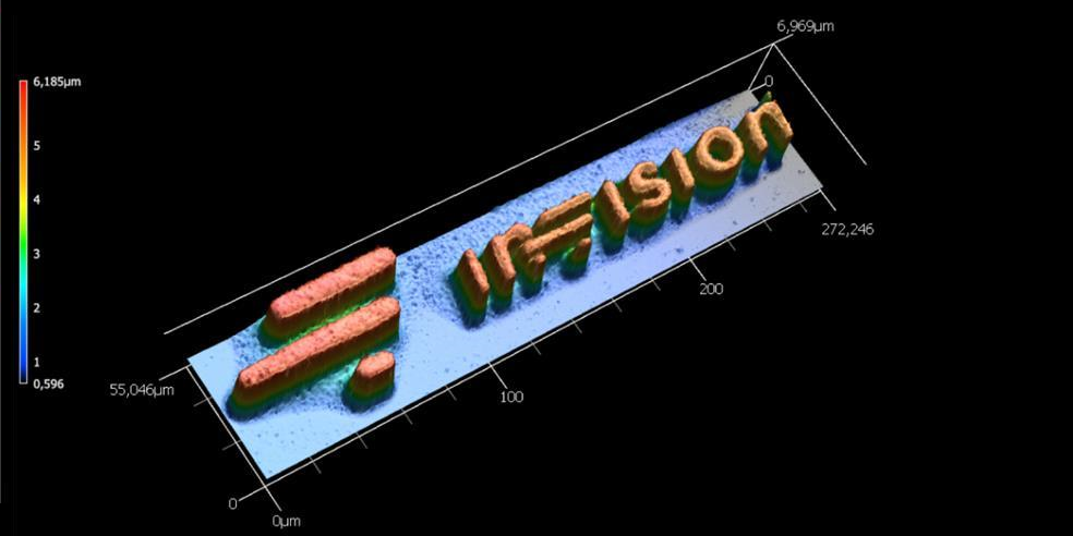
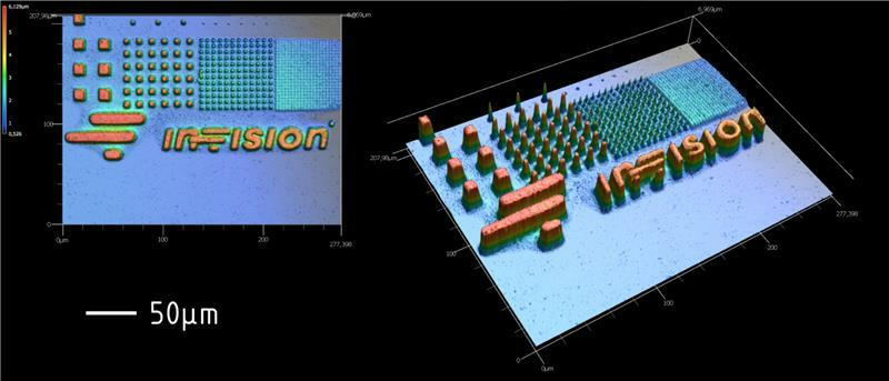
Where most 3D DLP projectors are limited to one-to-two-micron resolution, Das Gupta’s work requires something much smaller, in the sub-micron range. To achieve this exceptional precision and scaled down image, In-Vision is supplying a projector, based on a DLP9000-Chipset with a newly designed optical path to achieve the sub-micron resolution at a wavelength of 405 nanometers.
“The light engine is the key component of our process, and when you get to this sub-micron level resolution, it requires much greater precision,” Das Gupta said. “In-Vision is the only company willing to make this a reality by developing the world’s first sub-micron light engine for 3D-printing.”
With funding from the Indian Ministry of Electronics & Information, Das Gupta and In-Vision have partnered with J Group Robotics to collaborate and build the printer. The group meets frequently to collaborate on technical challenges and align on design and specifications for the printer, with an anticipated completion date of December 2023. Das Gupta says he expects the first optical component to be produced in Spring 2024.
Solving the Supply Chain Challenge
In addition to producing miniaturized photonic devices for AR/VR headsets, SLR cameras and smartphones, this sub-micron capability has broader applications for micro lenses in several other exciting areas. For example, the technology can be used to produce hydrogels and biopolymers for use in contact lenses, biosensors for detecting COVID-19 and other pathogens with a very low concentration of material through spectral analysis, and other applications in the semiconductor industry.
“3D-printing has taken over many other manufacturing processes, the only thing left is printing in submicron resolution,” Das Gupta said. “This technique has the potential to reduce the cost and drive drastic change in the semiconductor industry by eliminating the clean room requirement and making production much faster.”
In addition, Das Gupta says, “It also reduces the carbon footprint of the entire production process and could dramatically improve supply chain resiliency, allowing companies to produce and procure chips much closer to home.”
To learn more about Das Gupta’s work, visit http://iap.iisc.ac.in/people/tapajyoti/, and for more information on In-Vision’s high-resolution, high-performance light engines for 3D-printing, visit https://in-vision.at/.

Biography (source: IAP – IISc Bangalore)
Tapajyoti Das Gupta obtained his BSc and Btech in Physics and Radio physics from University of Calcutta in 2006 and 2009.
MSc in nanoscience from École Polytechnique (l’X) in 2012 and PhD in Condensed Matter Physics lab (PMC) from the same institute in 2015 under Prof. Thierry GACOIN and Alistair ROWE. He then joined prof. Fabien Sorin’s lab of Fiber Optics and Photonics Devices (FIMAP) in École Polytechnique Fédérale de Lausanne (EPFL) during 2015 December-2019 November. He also served in the Electrical Engineering department in Indian Institute of Technology, Kanpur (IITK) for five months from January 2020 to May 2020, before joining the Department of Instrumentation and Applied Physics in July 2020.
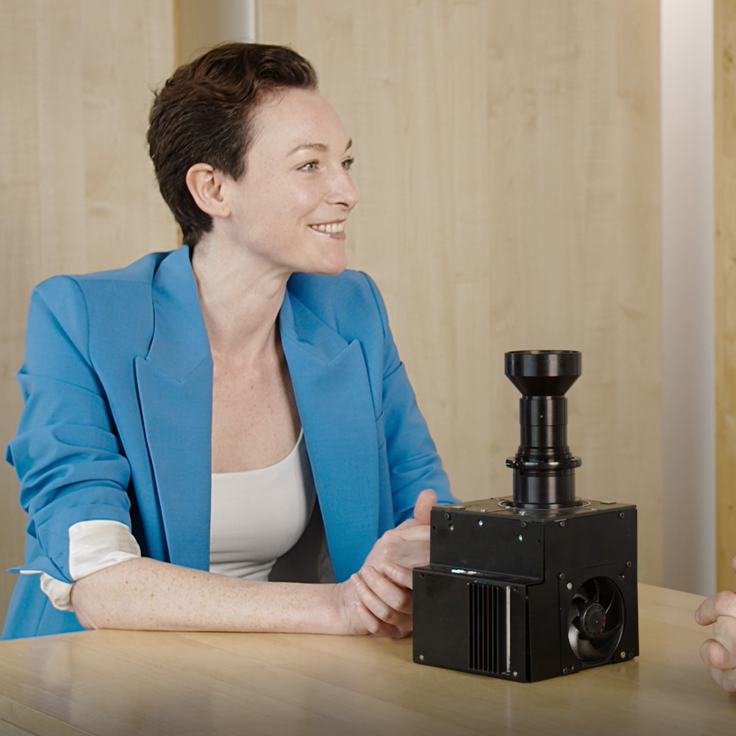
Video: DLP UV Projectors from IN-VISION
Follow Maggie Childs through the production line of In-Vision and learn more about Light Engines.
