Maskless Lithography
Maskless lithography is a modern approach to photonic patterning that replaces traditional mask-based exposure methods with dynamic, pixel-based projection using DLP® technology. Instead of producing fixed contrast masks for each design iteration, digital light engines generate precise exposure patterns directly onto photoresist-coated substrates - in real time and at high resolution.
This approach significantly reduces setup and tooling costs, eliminates the need for photomask production, and enables rapid design iteration. Particularly in small- and mid-volume manufacturing environments, maskless lithography offers a more flexible, cost-efficient path to production.
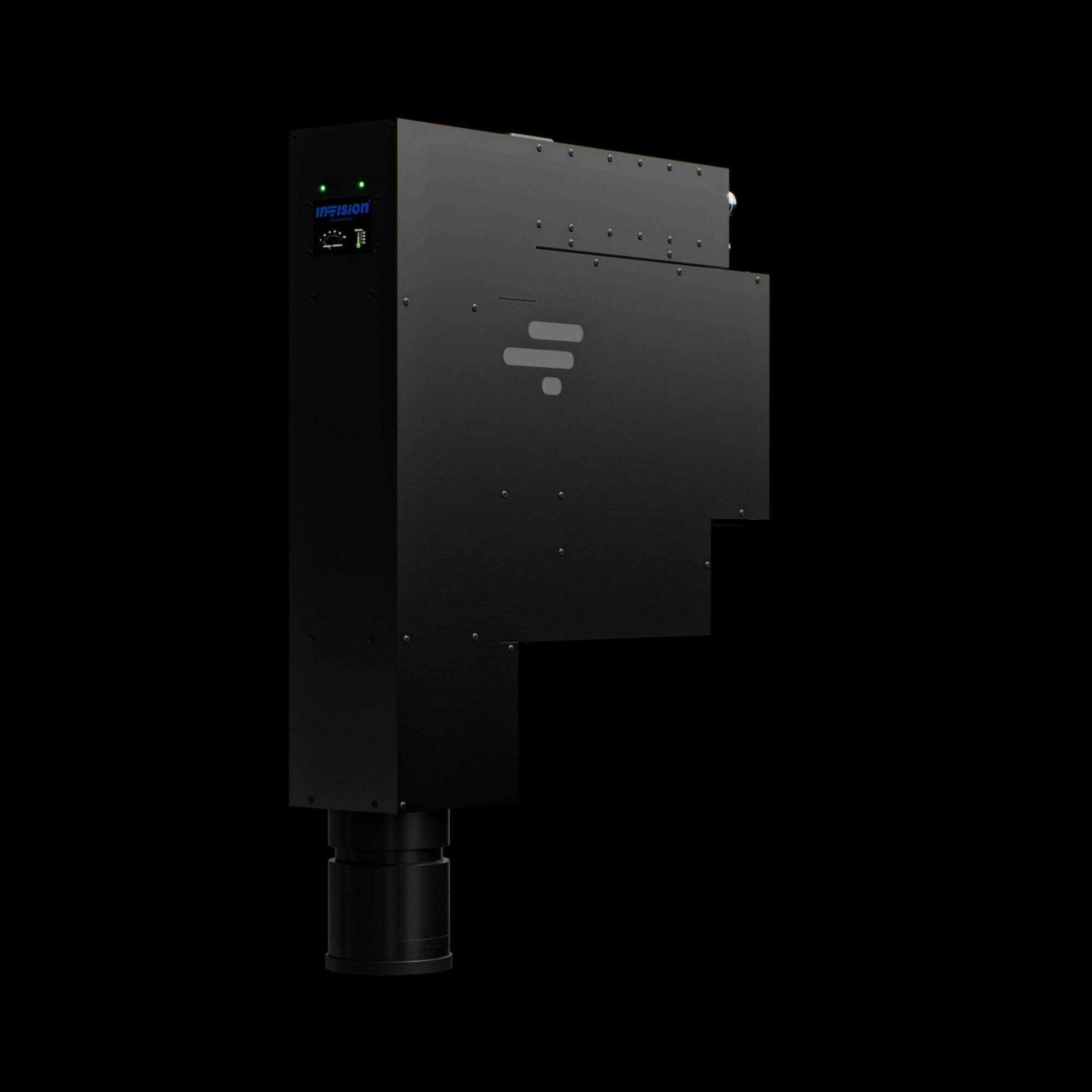
In-Vision’s high-performance UV light engines are built around this principle: by projecting millions of individually controllable pixels, we achieve outstanding image fidelity and alignment precision - even in the single-digit micrometer range. The high native pixel count of our systems ensures both fine feature resolution and uniform intensity distribution across large exposure fields.
As the demand for flexible and scalable lithographic tools grows, maskless systems offer an increasingly attractive complement - or even alternative - to traditional mask-based photolithography.
Appliation Areas
PCB Manufacturing
Direct imaging for multilayer PCBs, HDI, and IC substrates – enabling precise alignment and cost-effective scaling.
Advanced Packaging
Flexible exposure systems for RDL, interposers, and fan-out wafer-level packaging (FOWLP) with micron-level accuracy.
MEMS and Photonic Devices
High-precision projection systems for integrated photonics, optical sensors, and micro-electro-mechanical systems.
Custom UV Illumination for Direct Exposure Applications
Tailored light engines for production, laser structuring support, and emerging direct-write technologies.


IN-VISION's Maskless Lithography Solution
While maskless lithography has become a proven alternative for PCB imaging, solder masks, and direct-write exposure systems, its advantages also extend into advanced packaging, flat panel displays, and wafer-level lithography. In-Vision has successfully adapted this technology for silicon wafer applications requiring critical dimensions below 2 µm - pushing the limits of what's possible with digital optics. As the demand for flexible and scalable lithographic tools grows, maskless systems offer an increasingly attractive complement - or even alternative - to traditional mask-based photolithography.
Explore PANDIA