MEMS and Photonic Devices
MEMS and photonic components are defined by their complexity: dense features, layered architectures, and extreme precision. Traditional lithography meets these needs at high cost and long lead times. Maskless lithography offers a powerful alternative—combining flexibility with production-grade accuracy.


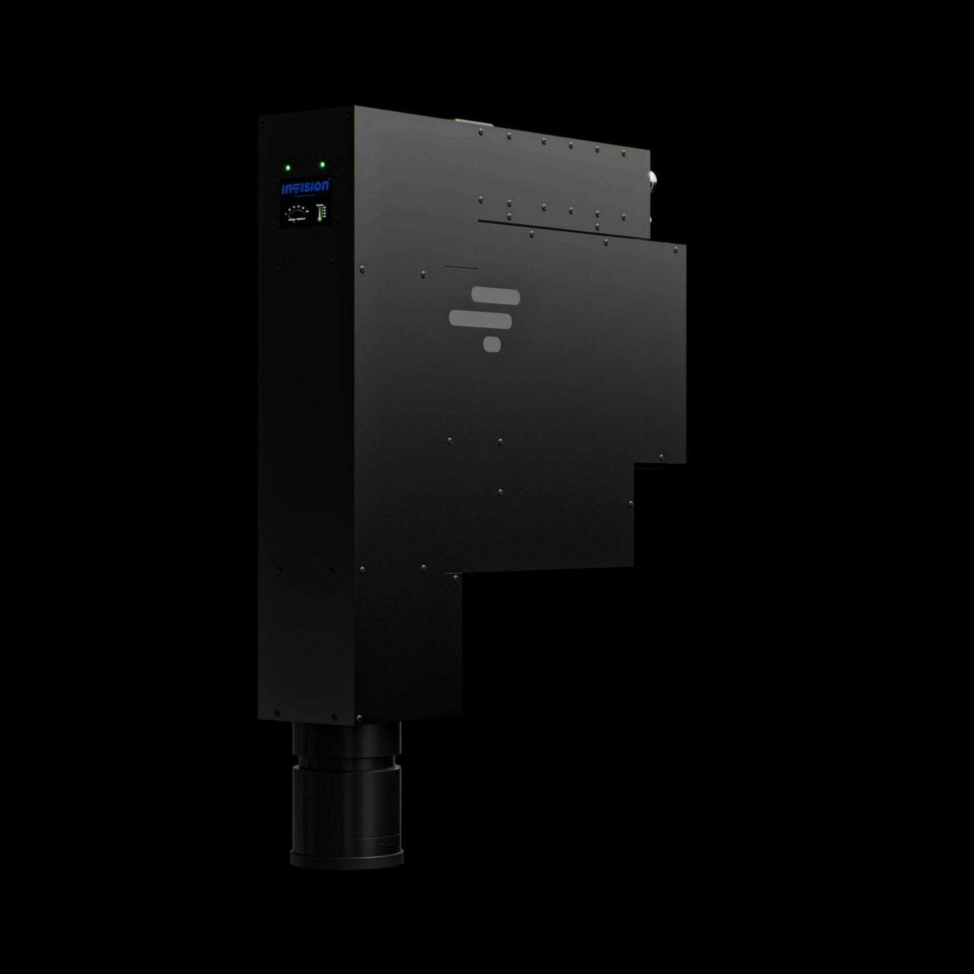
With In-Vision’s PANDIA Light Engine, exposure patterns are projected directly onto the substrate using DLP® technology. This eliminates the need for physical masks and allows designs to be changed instantly via software - enabling agile prototyping, faster development cycles, and scalable low- to mid-volume manufacturing for MEMS and integrated photonic devices.
Why It’s a Game-Changer
- High Design Flexibility
From waveguide geometries to micro-mechanical components, complex structures can be patterned without tooling changes or physical masks. - Accelerated Development
Research and pilot production benefit from rapid design iteration - with no delay for photomask fabrication or approval. - High Pattern Fidelity at Micron Scale
PANDIA delivers image-plane resolutions down to 2 µm, supporting the fine structures needed in photonic integrated circuits and MEMS arrays. - Software-Based Masking with No Tooling Costs
Design changes are made instantly, with no mask production, handling, or alignment procedures required. - Lower Total Cost of Ownership
Especially in short-run, high-value production, maskless workflows dramatically reduce upfront investment and improve ROI. - Deeper Process Capability through Extended DOF
Thanks to its advanced telecentric optics, PANDIA offers a high depth of field - which supports more complex multilayer lithography. This enables precise patterning across stacks of optical or mechanical layers, improving process latitude and integration density.
Why Us?
In-Vision’s PANDIA Light Engine is purpose-built for the precision and adaptability required in MEMS and photonic device fabrication.
- High Native Resolution with Upgrade Path to 4K
From WQXGA to true 4K (4096×2176 pixels), PANDIA offers pixel sizes down to 2 µm in the image plane, with excellent contrast and edge definition. - Deep DOF for Multilayer Patterning
The optical system provides a consistently sharp image across a broader vertical range, ideal for building up multi-layer photonic or MEMS structures without intermediate re-focusing. - Multi-Wavelength UV Compatibility
With up to three independently controlled channels (e.g. 365 nm, 385 nm, 405 nm) and up to 12 W per channel, PANDIA supports multiple resist chemistries and process variations. - Robust Architecture with Industrial Integration
FPGA-controlled with ~7 GB onboard memory, high-speed interfaces (GigE, PCIe), and modular LED units - ready for both lab use and production deployment.
Ideal Applications
- Integrated Photonics
Custom waveguides, splitters, and couplers on Si or InP platforms. - MEMS Devices
Precision patterning for accelerometers, pressure sensors, and microactuators. - Micro-Optics & DOE Fabrication
Production of lenslets, gratings, and structured optical elements. - Layered Photonic Architectures
Stepwise fabrication of multi-level waveguide and photonic circuit designs.
In summary, In-Vision’s PANDIA combines single-digit-micron resolution with a deep depth of field and modular control — making it the ideal solution for developing and producing advanced MEMS and photonic devices without the limitations of mask-based lithography.
