MEMS and Photonic Devices


MEMS and photonic components are defined by their complexity: dense features, layered architectures, and stringent requirements on alignment and edge precision. In classical lithography, these demands are often met with high cost and long lead times due to rigid mask-based workflows. Maskless lithography offers a powerful alternative - one that combines high flexibility with production-grade precision.
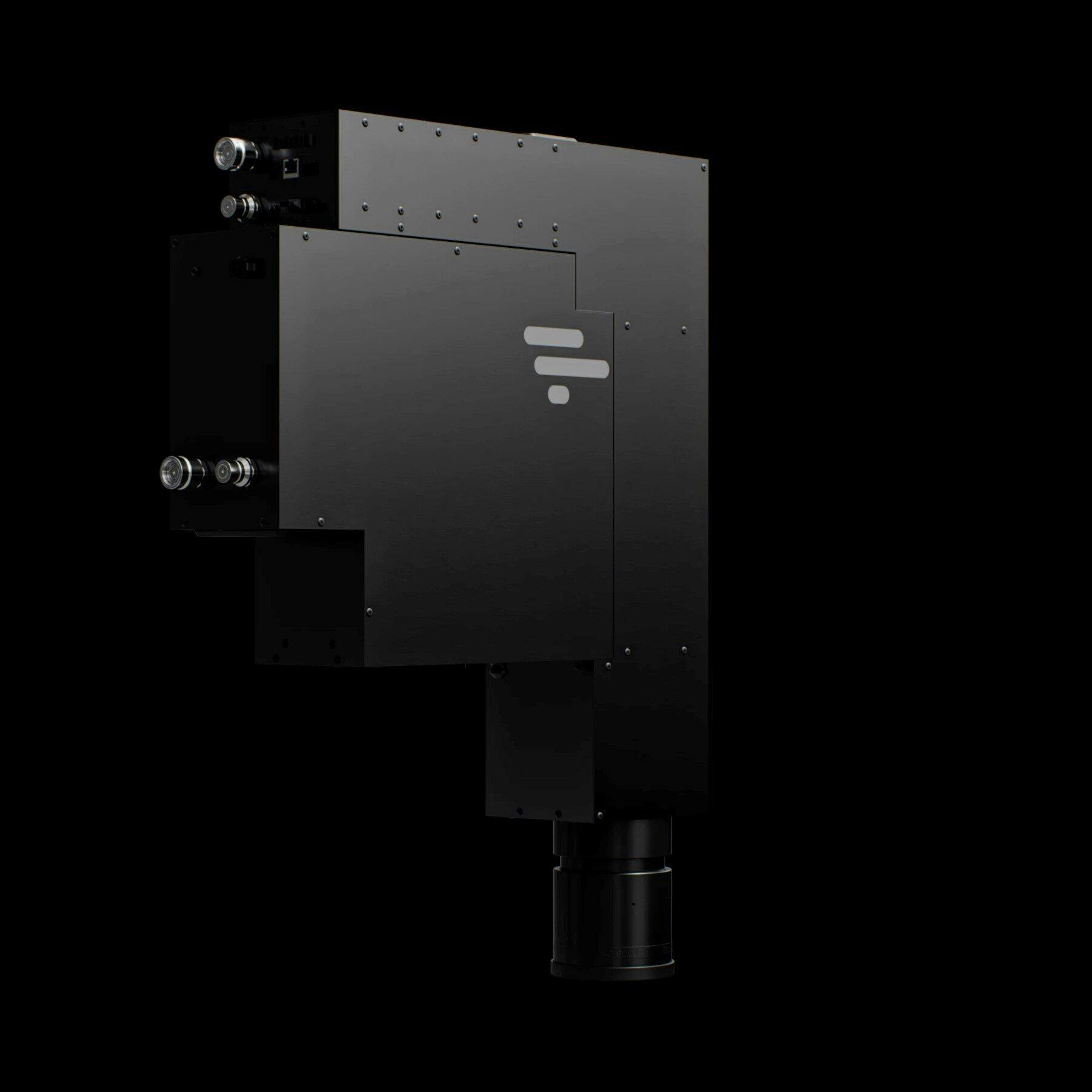
With In-Vision’s PANDIA Light Engine, exposure patterns are projected directly onto the substrate using DLP® technology. This eliminates the need for physical masks and allows designs to be changed instantly via software - enabling agile prototyping, faster development cycles, and scalable low- to mid-volume manufacturing for MEMS and integrated photonic devices.
Why It’s a Game-Changer
- High Design Flexibility
From waveguide geometries to micro-mechanical components, complex structures can be patterned without tooling changes or physical masks. - Accelerated Development
Research and pilot production benefit from rapid design iteration - with no delay for photomask fabrication or approval. - High Pattern Fidelity at Micron Scale
PANDIA delivers image-plane resolutions down to 2 µm, supporting the fine structures needed in photonic integrated circuits and MEMS arrays. - Software-Based Masking with No Tooling Costs
Design changes are made instantly, with no mask production, handling, or alignment procedures required. - Lower Total Cost of Ownership
Especially in short-run, high-value production, maskless workflows dramatically reduce upfront investment and improve ROI. - Deeper Process Capability through Extended DOF
Thanks to its advanced telecentric optics, PANDIA offers a high depth of field - which supports more complex multilayer lithography. This enables precise patterning across stacks of optical or mechanical layers, improving process latitude and integration density.
Why Us
In-Vision’s PANDIA Light Engine is purpose-built for the precision and adaptability required in MEMS and photonic device fabrication.
- High Native Resolution with Upgrade Path to 4K
From WQXGA to true 4K (4096×2176 pixels), PANDIA offers pixel sizes down to 2 µm in the image plane, with excellent contrast and edge definition. - Deep DOF for Multilayer Patterning
The optical system provides a consistently sharp image across a broader vertical range, ideal for building up multi-layer photonic or MEMS structures without intermediate re-focusing. - Multi-Wavelength UV Compatibility
With up to three independently controlled channels (e.g. 365 nm, 385 nm, 405 nm) and up to 12 W per channel, PANDIA supports multiple resist chemistries and process variations. - Robust Architecture with Industrial Integration
FPGA-controlled with ~7 GB onboard memory, high-speed interfaces (GigE, PCIe), and modular LED units - ready for both lab use and production deployment.
Ideal Applications
- Integrated Photonics
Custom waveguides, splitters, and couplers on Si or InP platforms. - MEMS Devices
Precision patterning for accelerometers, pressure sensors, and microactuators. - Micro-Optics & DOE Fabrication
Production of lenslets, gratings, and structured optical elements. - Layered Photonic Architectures
Stepwise fabrication of multi-level waveguide and photonic circuit designs.
In summary, In-Vision’s PANDIA combines single-digit-micron resolution with a deep depth of field and modular control — making it the ideal solution for developing and producing advanced MEMS and photonic devices without the limitations of mask-based lithography.