Maskless Lithography for Advanced Packaging


Maskless lithography offers a powerful alternative to classical photomask-based exposure processes in advanced packaging. With growing demands for ultra-fine features, tighter interconnect pitches, and heterogeneous integration, conventional methods often struggle to keep pace - particularly when agility, cost-efficiency, and design iteration are critical. In-Vision’s digital light engines, such as PANDIA, directly expose high-resolution UV patterns onto wafer-level or panel-level substrates, removing the need for static photomasks. This makes the process more adaptable, scalable, and cost-effective for RDL, interposers, and fan-out wafer-level packaging (FOWLP).
Why It's A Game Changer
- No Photomasks Required
Conventional workflows rely on dedicated masks for every packaging layer - a rigid and expensive constraint. Maskless lithography enables software-based pattern changes, eliminating tooling delays and costs. - Ideal for Complex and Multi-Layer Packages
Whether dealing with warpage, alignment variation, or low-volume trial runs, maskless projection offers unmatched process flexibility.
The Competitive Advantage Over Masks
- Micron-Scale Patterning for Advanced Packaging Features
With pixel-level control, PANDIA supports feature sizes below 10 µm and edge definition suitable for next-gen RDL, interposers, and photonic I/O structures. - Lower Cost of Ownership
No mask production means lower setup costs, reduced inventory, and faster yield learning - ideal for advanced prototyping and early production. - Adaptability for Warped or Panelized Substrates
Scrollable exposure and dynamic stitching compensate for complex geometries, making it ideal for large panel-level packaging workflows. - Future-Proof Technology
As packaging requirements evolve, PANDIA can scale - from WQXGA to native 4K resolution - and adapt to new materials and exposure strategies.
Why Us
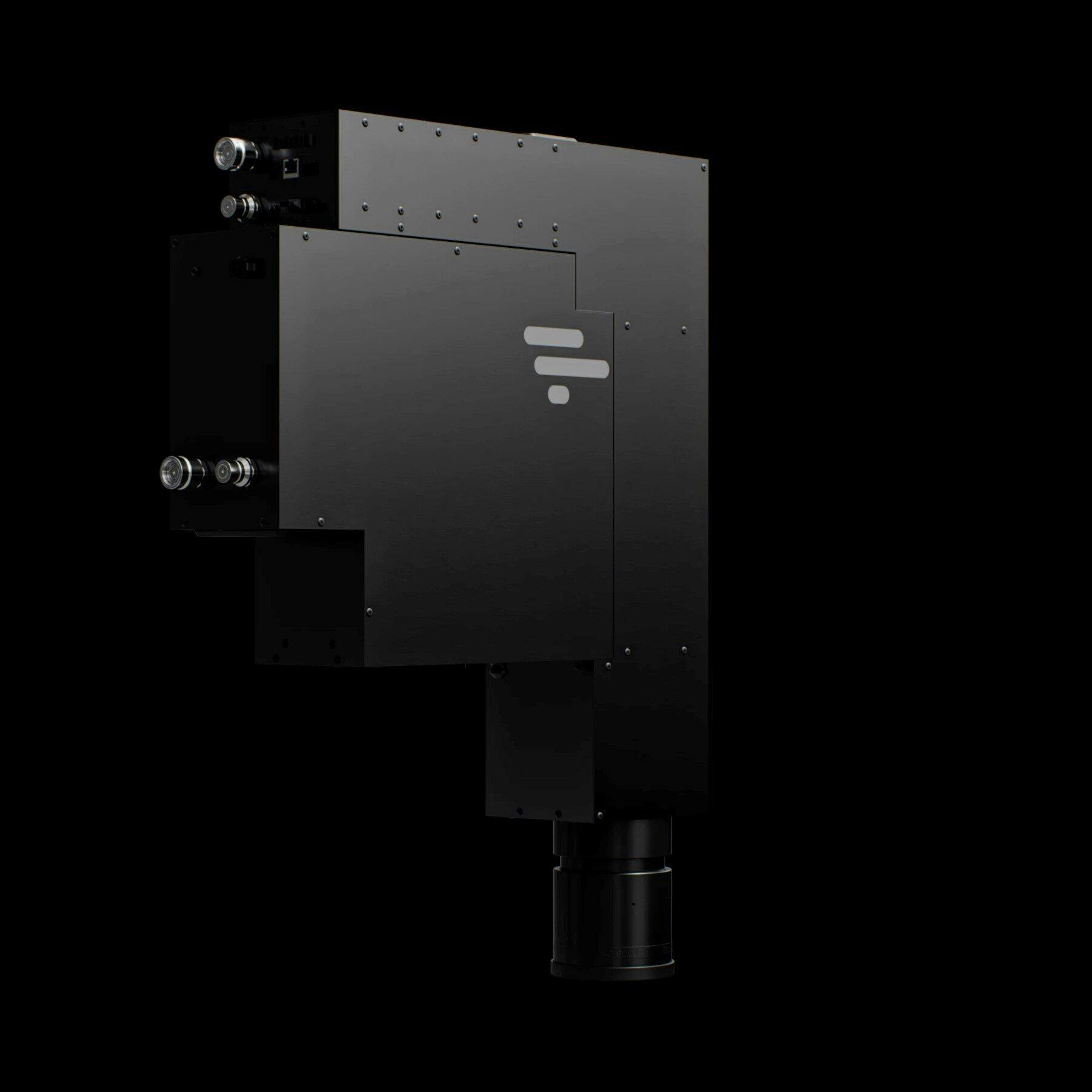
In-Vision’s PANDIA Light Engine is purpose-built for the rigors of advanced packaging lithography - combining resolution, modularity, and industrial robustness.
- Native High Resolution & Pixel-Level Accuracy
With WQXGA resolution upgradeable to native 4K (4096×2176), PANDIA achieves pixel sizes down to 2 µm in the image plane - essential for fine-line redistribution layers and dense interconnects. - Large Exposure Area via Multi-Exposure & Stacking
PANDIA supports continuous scrolling exposure and multi-engine stacking, enabling precise, large-format imaging across wafers and panels. - Multi-Wavelength UV Capability
With up to three UV wavelengths (e.g. 365/385/405 nm), independently addressable and up to 12 W per channel, PANDIA supports multilayer resist processes and functional ink deposition. - Industrial-Grade Throughput & Control
An onboard FPGA with ~7 GB memory enables fast image streaming via GigE or optical PCIe. The system integrates seamlessly into automation workflows, and features field-replacement LED modules and real-time monitoring via onboard HMI.
Ideal Applications
- Fan-Out Wafer-Level Packaging (FOWLP)
Seamless imaging of redistribution layers and bump structures with fine-line precision. - 2.5D Interposers & Embedded Die
Supports dense interconnect structures and multi-material processing in heterogeneous integration platforms. - Wafer & Panel-Level Lithography
Scalable projection architecture adapts to both formats without process changes. - Photonic Packaging
High-resolution patterning for integrated optical components and waveguide layers.
In summary, PANDIA-powered maskless lithography offers a digitally agile, cost-effective, and precision-focused lithographic solution tailored for the evolving demands of advanced semiconductor packaging.