Maskless Lithography for PCB Manufacturing

August 2025

Teilen Sie diesen Inhalt:

Maskless UV lithography represents a transformative leap beyond conventional photomask-based exposure systems. Instead of relying on static contrast masks, In‑Vision’s digital Light Engines, such as PANDIA, dynamically project high-resolution UV patterns directly onto photoresist-coated PCBs - enabling on-the-fly design changes and near-zero setup cost. This flexibility dramatically reduces production expenditure and accelerates time-to-market, particularly for small- to mid-volume runs and prototyping.

Why It's A Game Changer

  • No Photomasks Required
    Traditional photolithography demands manufacturing a mask for every new PCB design- an expensive and time-consuming process. Maskless lithography eliminates this step entirely, slashing overhead and enabling iterative design workflows without penalty.
  • Dynamic Design Adaptation
    With maskless systems, pattern changes are software-driven. Manufacturers can instantly update design files without physical tooling, making it ideal for agile R&D, custom jobs, or fast-turn PCB runs.

The Competitive Advantage Over Masks

  • Ultra-Precise Patterning
    High native resolution enables single-digit micrometer fidelity, critical for HDI, fine-line PCBs, and cutting-edge packaging.
  • Reduced Cost & Greater Flexibility
    Eliminates the need for expensive mask production; perfect for agile manufacturing, small batches, and just-in-time processes.
  • High Throughput with Scalability
    Scrolling and stacking capabilities allow PANDIA to match or exceed traditional equipment throughput, while remaining modular and cost-effective.
  • Simplified Upgrades & Adaptability
    As DLP chipsets and optics evolve, PANDIA can be upgraded to higher native resolution (from 2K to real 4K), future-proofing your lithography setup

Why Us

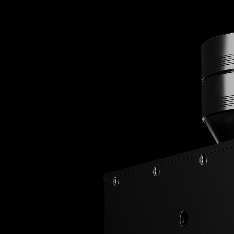
In-Vision’s flagship UV light engine, PANDIA, is engineered for maskless lithography and excels in demanding PCB manufacturing contexts:

  • Native High Resolution & Micron-level Accuracy
    Utilizing a high-resolution DLP chipset, PANDIA delivers WQXGA resolution, upgradeable to native 4K (4096×2176 pixels). Combined with telecentric optics, this achieves pixel pitches with single-digit micrometer precision, down to 2µm pixel resolution in the image plane.
  • Large Exposure Areas via Scrolling & Stacking
    PANDIA supports scrolling exposure, enabling continuous patterning over large substrate surfaces via multi-exposure. Multiple units can be stacked in parallel, facilitating seamless scaling to expansive boards
  • Powerful, Multi-Wavelength Illumination
    Equipped with two independently controllable UV LED modules (up to three colors), PANDIA enables multi-layer processing, multi-material compatibility, and functional solder mask deposition- delivering up to 12W per wavelength with robust water cooling. Its modular design allows hot-swappable LED modules, while an onboard HMI gives real-time diagnostic feedback
  • Industrial-Grade Performance & Customization
    With a built-in FPGA offering ~7GB memory, PANDIA provides onboard image buffering, high-speed data handling (via GigE or optical PCIe), and seamless integration points to existing software architecture.

Optional: Ideal Applications

  • Multilayer PCB & HDI Fabrication
    Ideal for high-density routing, microvias, and precision alignment across layers.
  • Solder Mask Deposition
    Enables accurate, defined UV-curable mask patterns with flexible color integration.
  • IC-Substrates & Packaging Structures
    Supports fine-feature RDL and fan-out wafer-level packaging in advanced electronics.
  • Prototyping & Short Runs
    Reduces costs and turnaround times dramatically compared to mask-reliant methods.